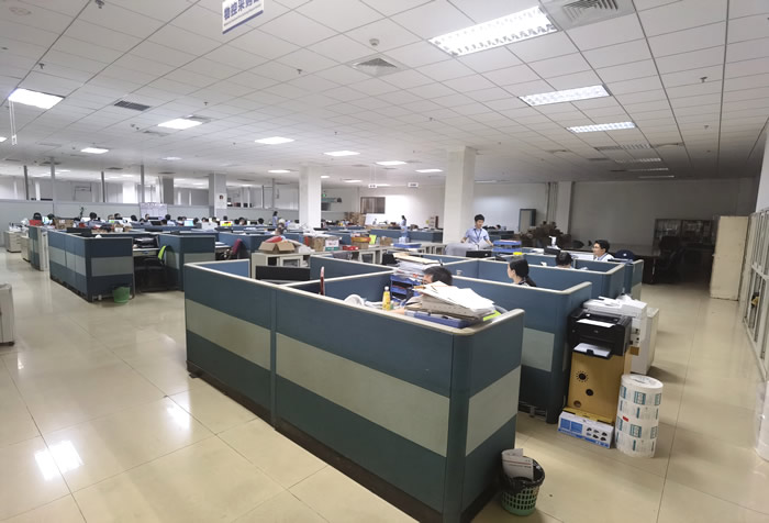
Runtek was established in 2018 and is located in Huizhou, China, close to Guangzhou and Shenzhen port, its predecessor, TJPCB was founded in 2001. Our main business is PCB research and development, production and sales. We have a capability of whole process production covering a variety of PCB types such as HDI, multilayer, rigid-flex, heavy copper board, medal based board, high frequency board, flex board and so on.
We supply clients with OEM or ODM or OBM services too. Email to our customer support for any inquiry, product samples. Welcome to get in touch with us.
Founded in
Employee
Factory Area
Yearly Output
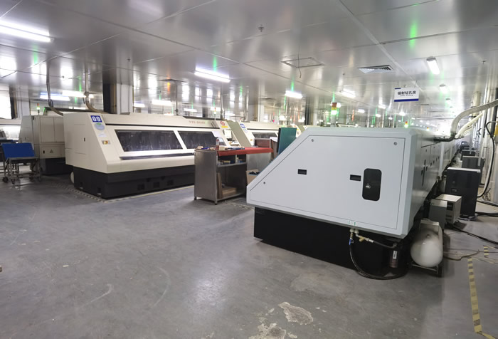
Runtek always holds the concept of “providing high-tech and high reliable PCB and service for the sustainable development of electronic technology with minimal resource consumption”. We will continue to strengthen the basic research and development and product development, enhance product competitive edge, increase the advanced equipment and production line input, improve production capacity, efficiency and automation level.
RunTek-Us | Other Company |
Four shots in each laser hole | Three shots in each laser hole |
0.1mm drill diameter | 0.075mm drill diameter |
Copper thickness 25-30 μm | Copper thickness 18 μm |
Japanese Laser exposure machine, 25 μm resolution, much reliable. | Traditional Film exposure machine, low yield, accuracy and stability. |